
MIT Model Detects Multiple Material Defects Without Damaging Samples
MIT researchers have built an AI model that identifies and measures up to six types of point defects in materials simultaneously using neutron-scattering data. The model, trained on 2,000 semiconductor materials, can detect defect concentrations as low as 0.2 percent without cutting into or otherwise damaging finished products.
The work addresses a longstanding problem in manufacturing. Engineers routinely introduce defects during production of semiconductors, steel, and solar cells to improve strength and electrical properties. But measuring what defects actually exist in finished materials has remained difficult.
"Existing techniques can't accurately characterize defects in a universal and quantitative way without destroying the material," said Mouyang Cheng, a PhD candidate in materials science and engineering who led the research. "For conventional techniques without machine learning, detecting six different defects is unthinkable."
Why Current Methods Fall Short
Engineers have many ways to introduce defects through doping, but they struggle with basic questions: What defect did they create, and in what concentration? Unwanted defects like oxidation can also form during synthesis.
Existing techniques each have narrow scope. X-ray diffraction and positron annihilation characterize only certain defect types. Raman spectroscopy identifies defect type but cannot directly measure concentration. Transmission electron microscopy requires cutting thin slices from samples.
The result is that manufacturers often run invasive quality tests on only a small percentage of products coming off production lines. This slow process limits their ability to catch defects across entire batches.
How the Model Works
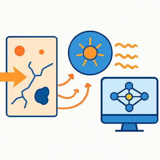
The researchers created a computational database of 2,000 semiconductor materials. For each material, they made two samples: one doped with defects and one without. They then measured the vibrational frequencies of atoms in each sample using neutron scattering.
The team trained a machine-learning model on these results using a multihead attention mechanism-the same approach used in large language models. The model learned to extract differences between defect-free and defective materials and predict which dopants were used and at what concentrations.
The researchers verified the model on experimental data from an electronics alloy and a superconductor material. They then deliberately introduced multiple defects to test its limits, finding it could handle up to six simultaneous defects.
"We were really surprised it worked that well," Cheng said. "It's very challenging to decode the mixed signals from two different types of defects-let alone six."
Path to Industry Adoption
The neutron-scattering technique that powered the model's training is powerful but difficult for manufacturers to deploy in their own quality-control labs. Access to neutron sources is limited and the equipment is complex.
Companies have already expressed interest and asked when the approach will work with Raman spectroscopy, a widely available technique that measures light scattering. The researchers plan to train a similar model using Raman data as their next step. They also intend to expand the approach to detect larger defects like grain boundaries and dislocations.
The research demonstrates a core advantage of AI for materials science: pattern recognition that exceeds human perception. To the naked eye, signals from different defects look nearly identical. AI can discern the differences and identify ground truth.
The work appears in Matter and was supported by the Department of Energy and National Science Foundation.
For researchers working with materials characterization and defect analysis, understanding AI applications in this space can open new possibilities for quality control and materials optimization. AI for Science & Research courses cover practical applications of machine learning in scientific workflows.
Your membership also unlocks: