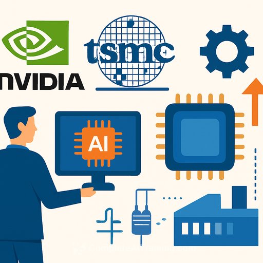
NVIDIA and TSMC Deploy AI Across Semiconductor Manufacturing
NVIDIA announced that TSMC is using accelerated computing and AI across semiconductor design and manufacturing operations, applying the technology to lithography, transistor simulation, process control, and wafer inspection. The partnership addresses a core problem: as chips advance to smaller nodes, the computational demands of moving designs into high-volume production have become one of the world's most complex challenges.
TSMC is deploying NVIDIA's CUDA-X libraries and specialized AI models to handle massive-scale simulations and real-time optimization across multiple manufacturing stages. The goal is measurable: improve turnaround time, energy efficiency, yield, and operational productivity in advanced fabs.
Where NVIDIA Technology Is Being Applied
Computational lithography: TSMC uses NVIDIA cuLitho for GPU-accelerated mask design. The library delivers 20-50% improvements in cost effectiveness or cycle time compared with CPU-based approaches, while maintaining the same cost of ownership.
Transistor and process simulation: NVIDIA cuEST accelerates electronic structure simulation for semiconductor material design. The library achieves 50x faster chemistry simulations on average.
Process control: TSMC uses NVIDIA cuML, a machine learning library, to accelerate large-scale analytics on GPUs. This allows the company to process hundreds of thousands of process parameters across thousands of manufacturing steps as inputs for machine learning models, reducing process variation.
Fab operations: NVIDIA H200 GPUs running CUDA-accelerated scheduling have improved TSMC's ability to manage complex production constraints. The result is streamlined production paths and higher fab productivity.
Defect inspection: TSMC uses NVIDIA Metropolis and the TAO Toolkit to improve defect classification using vision AI. The system detects nanometer-scale defects more accurately while reducing the need for repeated labeling and retraining as process conditions change.
Virtual Fab Planning
TSMC is exploring NVIDIA Omniverse libraries to build FabTwin, a virtual fab environment for testing process tool layouts and simulation workflows. The system lets engineers evaluate design scenarios digitally before physical implementation, identifying constraints earlier and reducing capital commitments before decisions are made.
Jensen Huang, NVIDIA founder and CEO, said TSMC is "bringing NVIDIA AI and accelerated computing into the fab itself, tackling some of the world's most complex design and manufacturing challenges with simulation, optimization and AI to improve speed, efficiency and yield for the next generation of chips."
C.C. Wei, TSMC chairman and CEO, said the partnership strengthens "our technology leadership and manufacturing excellence to support our customers' future products and success."
The partnership spans nearly three decades of collaboration between the two companies.
Professionals in operations and product development should understand that accelerated computing and AI are now embedded in core manufacturing processes - not as add-ons, but as essential tools for managing the computational scale of modern semiconductor production. AI for Operations and AI for Product Development are increasingly inseparable from competitive advantage in advanced manufacturing.
Your membership also unlocks: